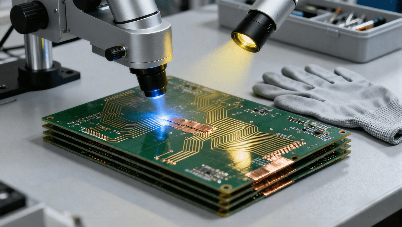
As the semiconductor industry races toward sub-5nm nodes, traditional mechanical dicing is hitting a hard ceiling. Enter laser cutting—the industry’s modern "optical scalpel." By merging advanced optics, ultra-precise control, and material science, laser technology is rewriting the rules for wafer fabrication and advanced packaging.
Here is how laser cutting is driving the next era of high-yield, precision manufacturing.
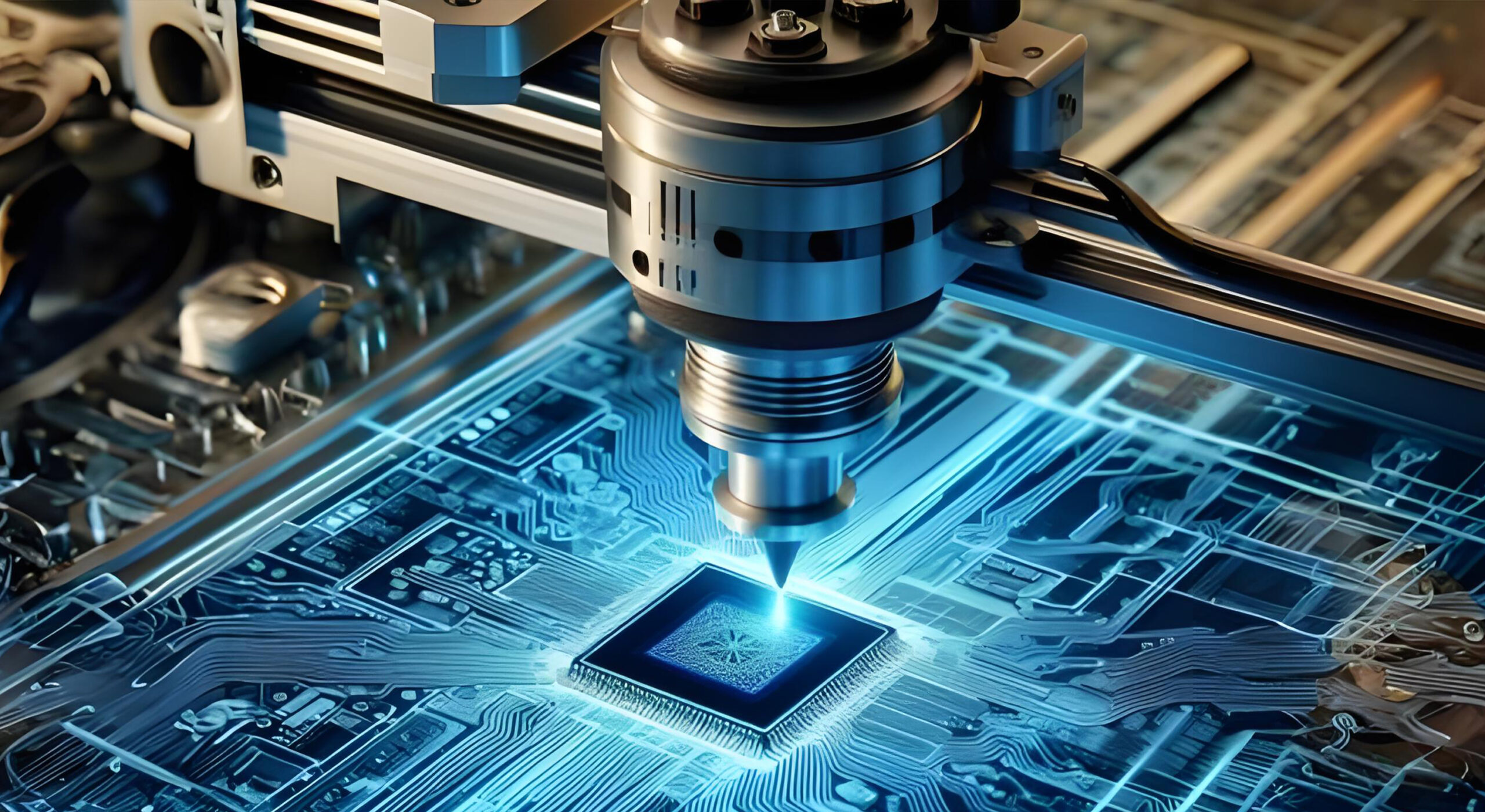
I. The Core Edge: 4 Ways Laser Disrupts Legacy Processing
By combining diode-pumped solid-state (DPSS) lasers with high-speed galvanometers, laser cutting delivers a quantum leap in accuracy and throughput over mechanical methods.
- Sub-Micron Precision: Achieves an accuracy of ±0.1 μm on hard, brittle substrates (Silicon, SiC). For ultra-thin wafers (~2 μm), femtosecond UV hybrid lasers keep edge chipping under 1 μm, perfect for complex MEMS and advanced ICs.
- True "Cold Processing": Ultra-short pulse (USP) lasers utilize cold ablation to remove material, restricting the Heat-Affected Zone (HAZ) to ≤0.5 μm. In SiC wafer production, this tech has pushed yields from 80% to 96% by eliminating thermal stress and micro-cracks.
- 5x to 10x Throughput Boost: On 6-inch SiC wafers, cutting speeds reach 5–10 mm/s, dropping per-wafer processing times under 10 minutes. Furthermore, multi-beam parallel processing boosts single-equipment capacity by 200%.
- Total Material Versatility: From sapphire and ceramics to GaAs and SiC, lasers cut them all. Notably, water-guided laser technology accelerates silicon cutting by 7–10x while entirely capturing dust, offering a cleaner, greener fab environment.
II. High-Value Application Scenarios
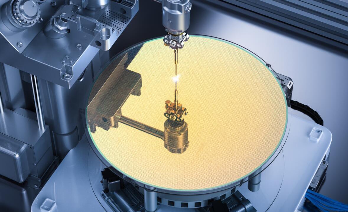
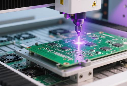
1. Wafer Dicing & Advanced Packaging (2.5D/3D IC)
- Stealth Dicing: Focusing the laser inside the substrate creates a modified layer for clean separation. This shrinks dicing streets to ≤20 μm, yielding more dies per 300 mm wafer.
- Fine-Wire Cutting: Precisely cuts 30 μm ultra-fine bonding wires in Flip Chip and WLCSP layouts. Backed by machine vision, alignment accuracy reaches a stellar ±5 μm.
2. Micro-Nanostructure Engineering
- Micro-Drilling: Drills 50 μm micro-holes on 0.05 mm Polyimide (PI) substrates with 1/10 the roughness of mechanical drills—crucial for 5G antenna arrays.
- 3D Sculpting: Uses helical scanning to engrave 80 μm wide grooves and 10×10 μm micro-pyramids on silicon for quantum chips and micro-optics.
3. Next-Gen Compound Semiconductors (SiC/GaN)
- Automotive-Grade SiC: UV picosecond lasers deliver crack-free dicing with a 90°±0.5° kerf taper and a smooth finish (Ra≤0.8 μm).
-
High-Frequency GaN: Achieves a sharp 10:1 aspect ratio in vertical structure etching for GaN-on-Si wafers, speeding up the miniaturization of RF communication chips.
III. Head-to-Head: Laser vs. Traditional Methods
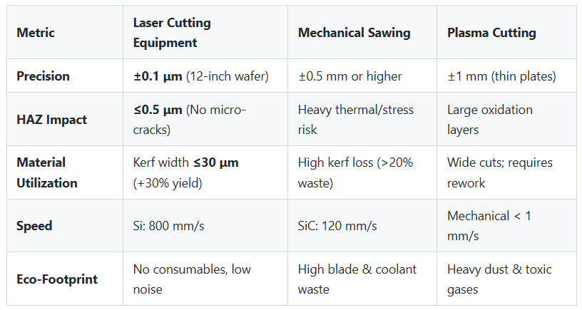
The Bottom Line: In third-generation semiconductor fabs, switching to laser processing slashes single-wafer processing costs by 40% while multiplying throughput fivefold.
IV. Future Outlook & Equipment Selection
Where is the Tech Heading?
- Pulse Evolution: Moving to attosecond-level (<100 fs) lasers for damage-free dicing on challenging substrates like GaN-on-Diamond.
- AI-Assisted Optimization: Toolpaths and laser parameters will auto-adjust via closed-loop AI algorithms based on real-time material feedback.
- Massive Multi-Beam Scales: Scaling up to 8–16 simultaneous beams to maximize throughput for large-diameter wafers.
Checklist for Buyers
- Match Precision to Substrate: Aim for ±0.5 μm for standard silicon; demand ±0.1 μm for third-gen power electronics (SiC/GaN).
- Pick the Right Source: Target UV lasers for ultra-fine structures, and picosecond/femtosecond configurations for ultra-fast "cold" dicing.
- Insist on Automation: Prioritize machines equipped with automatic machine vision alignment and self-optimizing software parameters.
V. Conclusion: Driving the Next Semiconductor Paradigm
The transition from mechanical sawing to laser cutting isn’t just an incremental upgrade—it is a manufacturing paradigm shift. By solving the legacy pain points of edge chipping, thermal stress, and throughput bottlenecks, lasers are actively unlocking the next generation of hardware required for 6G, electric vehicles, and quantum computing. As ultrafast pulses and AI-driven control converge, laser technology stands as the definitive cornerstone for high-yield, sustainable semiconductor fabrication.